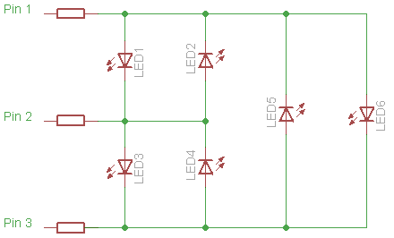
v0.1: 6 leds (3 pins), attiny45, phototrans, button, isp header (no battery) -- board done.
v0.1 -- code is the fails. I've been chasing this weird compiler bug for many days now.
So I milled and populated my eagle circuit and it works (well, the LEDs at least, haven't tested buttons / phototransistor). https://github.com/nouyang/pov-yoyo and http://fab.cba.mit.edu/classes/4.140/people/nancy.ouyang/Week11/Week11.html
 |
| eagle schematic I'm using the ng.lbr, fab.lbr, and the sparkfun libraries. More info here: http://academy.cba.mit.edu/tutorials/eagle/eagle_resources.html and the list of parts in fab.lbr: http://fab.cba.mit.edu/about/fab/inv.html |
 |
| board layout |
 |
| slightly cleaned up, colors inverted, for milling out on the roland modella in the MIT Media Lab shop. I export at 1000 dpi to be safe, and clean it up in the open-source and free GIMP image editor. |
 |
| powered off of USB for now. |
 |
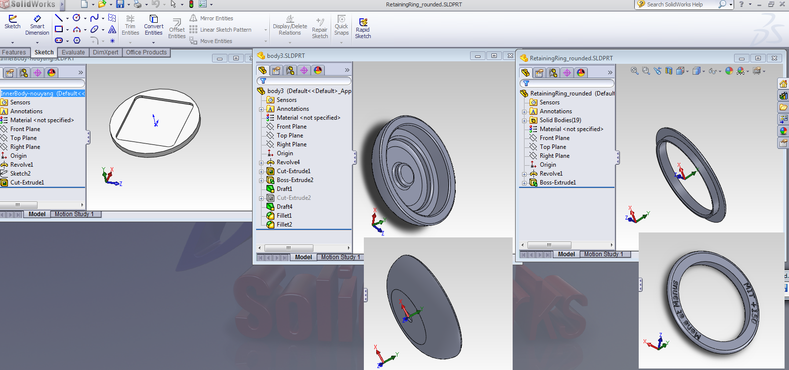
| The three parts that I 3d printed |
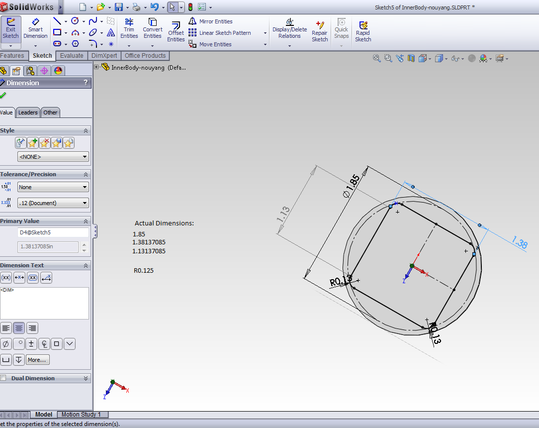
So yea, you can poke the eagle file on github and see that I simply drew a rectangle starting at the origin and then set the x2 and y2 coordinates according to the 2d solidworks measurements. (For more on spatial constraints and pcb layout, see http://orangenarwhals.blogspot.com/2011/11/how-to-design-pcbs-to-fit-cad-models.html)
I ended up approximating in Eagle the dimensions from the CAD file that I would need to fit inside the
 |
| inner body determines dimensions of board. Corners filleted due to concern over injection molding mold machinability, but turns out to be unwarranted (I think), next version will have sharp corners. |
I ended up approximating in Eagle the dimensions from the CAD file that I would need to fit inside the
After that I devolved into code misery at the down point of which I was wondering why I couldn't even copy code correctly. Turns out to be a makefile issue. See: http://orangenarwhals.blogspot.com/2011/11/crazy-compiler-bugs-avr-studios-avr-gcc.html
Anyway, so now I'm at the point where I can turn each LED on individually, I'm still trying to figure out my code bugs.
Oh right, this is after my realization last week that I don't understand any codes. Not even hello world codes. 0b000? 0x000? 0? char? int? huh?
So, I read up on bit operations stuff -^-^-
I recommend these for explaining the hello world code, which seems straightforward now (turn LED on! turn off!) but seemed completely foreign when I was trying to debug my code / write my own / mash together code from other people.
[1] http://fab.cba.mit.edu/content/tools/microcontrollers/c_for_microcontrollers.html
[2] http://www.arduino.cc/playground/Code/BitMath
[3] http://iamsuhasm.wordpress.com/tutsproj/avr-gcc-tutorial/
My code's here:
https://github.com/nouyang/pov-yoyo
and I'll run over some things I hadn't found clearly explained here.
0x designates hexadecimal, while 0b designates binary. These are fixed flags, similar to a plus or minus sign in front of a number. The actual values that matter come afterward.
So 0b0010 translates to, in decimal, two. And the compiler will assume that there are infinity zeros to the right (well, until 'till the size of the variable or constant at least, eg 0b00000010 for a byte = 8 bits), just as in decimal "2" and "00[...]002" are equivalent.
1 << LINE_A means 1 << 0 according to the #defines : This means "put a 1 shifted over 0 bits", aka 0b1 or 0b00000001
1 << 1 : 0b10, or 0b00000010
The "|" means bitwise OR, aka I add the two numbers together to get
0b00000011 -- that is, DDRB pins 1 and 2 are both outputs and everything else is in high impedance mode. To be safe, since I am using 6 LEDs on 3 pins
and therefore cannot have uncertainty about whether the unused pin is in high impedance (input) mode or output mode, I explicitly state with
& ~(1<<LINE_C) that pin 7 (on the attiny45, see datasheet which tells me that pin7 corresponds to index 2 on DDRB -- hence #defines LINE_C 2) must be in high impedance mode.
See [1] for an explanation of what & ~(a 1 at the appropriate index)
I'm not certain this is necessary, since in my case I explicitly say "DDRB = 0b011" later in the code rather than saying "DDRB |= 0b011" which would have left high any unspecified pins that were originally high, but I'd rather put it in here than risk wondering if my bugs are because of this.
Thus, an equivalent led_dir array could have said led_dir = {0b001, 0b011, [...]}.
C Resources:
Anyway, so now I'm at the point where I can turn each LED on individually, I'm still trying to figure out my code bugs.
Oh right, this is after my realization last week that I don't understand any codes. Not even hello world codes. 0b000? 0x000? 0? char? int? huh?
So, I read up on bit operations stuff -^-^-
I recommend these for explaining the hello world code, which seems straightforward now (turn LED on! turn off!) but seemed completely foreign when I was trying to debug my code / write my own / mash together code from other people.
[1] http://fab.cba.mit.edu/content/tools/microcontrollers/c_for_microcontrollers.html
[2] http://www.arduino.cc/playground/Code/BitMath
[3] http://iamsuhasm.wordpress.com/tutsproj/avr-gcc-tutorial/
My code's here:
https://github.com/nouyang/pov-yoyo
and I'll run over some things I hadn't found clearly explained here.
0x designates hexadecimal, while 0b designates binary. These are fixed flags, similar to a plus or minus sign in front of a number. The actual values that matter come afterward.
So 0b0010 translates to, in decimal, two. And the compiler will assume that there are infinity zeros to the right (well, until 'till the size of the variable or constant at least, eg 0b00000010 for a byte = 8 bits), just as in decimal "2" and "00[...]002" are equivalent.
#define LINE_A 0
#define LINE_B 1
#define LINE_C 2
//DDRB direction config for each LED (1 = output) //in or output
const char led_dir[6] = {
( 1<<LINE_B | 1<<LINE_A & ~(1<<LINE_C)), //LED 0
( 1<<LINE_A | 1<<LINE_B & ~(1<<LINE_C)), //LED 1
[...]
};
//PORTB output config for each LED (1 = High, 0 = Low) //hi or loWhat do these lines mean? Well,
const char led_out[6] = {
( 1<<LINE_B & ~(1<<LINE_A)), //LED 0
[...]
};
1 << LINE_A means 1 << 0 according to the #defines : This means "put a 1 shifted over 0 bits", aka 0b1 or 0b00000001
1 << 1 : 0b10, or 0b00000010
The "|" means bitwise OR, aka I add the two numbers together to get
0b00000011 -- that is, DDRB pins 1 and 2 are both outputs and everything else is in high impedance mode. To be safe, since I am using 6 LEDs on 3 pins
 |
| http://en.wikipedia.org/wiki/Charlieplexing for more info |
& ~(1<<LINE_C) that pin 7 (on the attiny45, see datasheet which tells me that pin7 corresponds to index 2 on DDRB -- hence #defines LINE_C 2) must be in high impedance mode.
See [1] for an explanation of what & ~(a 1 at the appropriate index)
I'm not certain this is necessary, since in my case I explicitly say "DDRB = 0b011" later in the code rather than saying "DDRB |= 0b011" which would have left high any unspecified pins that were originally high, but I'd rather put it in here than risk wondering if my bugs are because of this.
Thus, an equivalent led_dir array could have said led_dir = {0b001, 0b011, [...]}.
C Resources:
- quick refresher: http://cslibrary.stanford.edu/101/EssentialC.pdf
- reference card: http://www.digilife.be/quickreferences/QRC/C%20Reference%20Card%20(ANSI)%202.2.pdf
- another "short" intro http://claymore.engineer.gvsu.edu/~steriana/226/C.CheatSheet.pdf
- https://github.com/nouyang/pov-yoyo
- 3 pins, 6 LEDs. charlieplexed pov
is based off of:
Charlieplexing code:- http://b2ben.blogspot.com/2011/02/diving-into-microcontrollers-my-tiny.html
- charlieplexed grid display
- (the code: https://github.com/benbrandt22/TinyLife5) in C
- And many thanks to Josh Gordonson of olopede.com: who have a
- attiny13, non charlieplexed, 5 pin arrangement: C code
- https://github.com/zbanks/muffinc/blob/master/code/upov/main.c
- My class http://academy.cba.mit.edu/classes/output_devices/index.html -- the makefile (which is BAD! missing a "-j .data" for avr-obj copy, leads to subtle bugs), schematic for inspiration,
- C code, grid charlieplexing
- http://www.wayneandlayne.com/projects/blinky/design/ (which already uses the blinking monitor with light sensor data transmission, _sigh_ but yay it is awesome!)
- 8 pins, 8 LEDs (direct drive). asm.
- The code: https://github.com/wayneandlayne/blinky/blob/master/pov/blinky_pov.asm
- Thanks to http://tomscircuits.blogspot.com/2009/06/nano-pov.html for giving me my first successful experience with PoV.
- 4 pins 8 LEDs (charlieplexed). asm.
- https://docs.google.com/#folders/0B_acb-AcSkXYY2Q4MzA0Y2ItM2Y2Ny00NjRkLTkyYjItMWRjMTI3MTFiNjlm
- one boring video if you want to see effects of changing speed without sensors and what it looks like not moving. due to low duty cycle from charlieplexing, and using green instead of red LEDs which are in general brighter for same amount of current, it's very hard to see in room lighting so this is in the dark
https://picasaweb.google.com/113942194695013581888/PoVYoyoPersistenceOfVision#5681150271712191538


No comments:
Post a Comment