Me: if I want to make a board in eagle which fits inside a shape that I have a solidworks model of (I only care about 2d for now). It's pretty straightforward, so I can do the oldskool from x1 to x2 thing, but what if it were more complicated? Is the only way to do this export an image in solidworks and make a library part of it, or use some import_bmp script and trace over it in eagle, or something crazy? I guess the opposite is easier, show only the board, export image, import into solidworks, and trace it... What if I cared about 3d? Is eagle just have zero support for this?
Charles Guan:
Also, if you want to make a board of a certain shape in Eagle, it's a terrible pain. I was in fact just messing with this tool yesterday:
http://www.micromagicsystems.com/#/dxf-converter/4523812840
What I did was make a solid model of the plan of the board (sketch > extrude), then laid it out in a DXF drawing as if I were waterjetting it. If you just export a sketch as a DXF you have to exclude things like dimensions. The tool just imports every DXF entity into the .brd file on the Dimension layer.
Example board outline: http://etotheipiplusone.net/pics/moter/nicesensor3.png
If your board has internal slotting and stuff it will import that too.
John David Cranor:
cross platform one: http://fab.cba.mit.edu/classes/MIT/863.09/people/cranor/How_to_Make_%28Almost%29_Anything/David_Cranor/Entries/2009/11/16_Week_9__Output_Devices_files/DXF2SCR.C
In 3d, I have no idea, but check out this post:
http://sketchupdate.blogspot.com/2011/09/visualizing-circuit-boards-with.html
If only Sketchup were parametric...
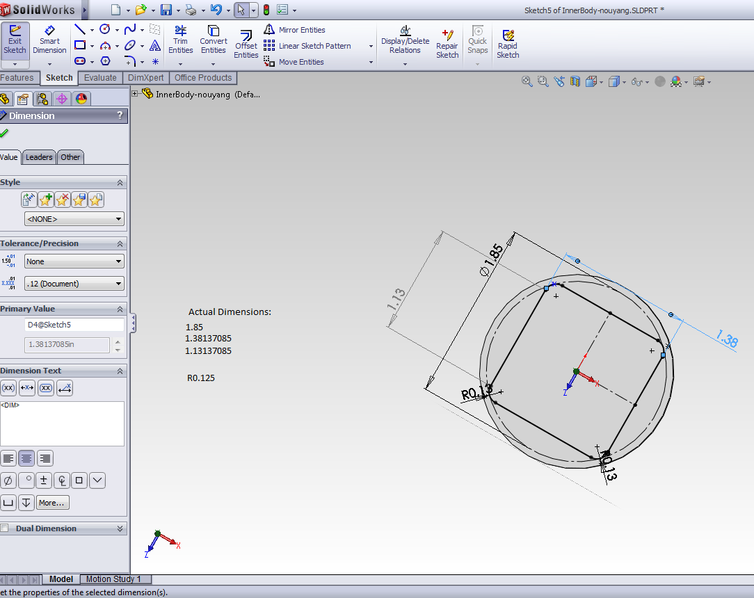
You can poke the eagle file on github (https://github.com/nouyang/pov-yoyo > eagle-board > .brd) and see that I simply drew a rectangle starting at the origin and then set the x2 and y2 coordinates according to the 2d solidworks measurements. For my prototype, I didn't even end up using that board outline -- I sheared off the excess copperclad and sanded* the pcb where my shearing was file until the pcb fit inside, and then used rolled up masking tape to keep it in 'cos I sanding failed past pressfit tolerances.
 |
FR1 versus FR4 copperclad:
The copper-clad we use in MAS.863 is FR1 Phenolic Paper, instead of the standard FR4 Epoxy Glass which is what you'll probably find on ebay if you search "pcb copperclad". Tiny particles of glass in the air make your lungs sad and result in increased cancer risk over time, so if you're milling boards or sanding them a lot you want to go with FR1. There are disadvantages which make FR4 preferred for Real Boards which are fine for DIY boards -- fr4 has less heat tolerance, delaminates easier, and cracks more easily -- see http://www.electronicspoint.com/paper-phenolic-pcb-t136758.html).
(For more info, see http://en.wikipedia.org/wiki/Printed_circuit_board;
for our fr4 supplier, see http://academy.cba.mit.edu/classes/electronics_production/index.html)
=====
Yes, I'm splitting my giant!update for today into 3 posts.
=====
(p.s. if you don't know what eagle is, it's free pcb layout software, older version layout tutorial: http://www.sparkfun.com/tutorials/109
schematic tutorial: http://www.sparkfun.com/tutorials/108
more resources (including eagle libraries) here: http://academy.cba.mit.edu/tutorials/eagle/eagle_resources.html,
and the list of parts for fab.lbr: http://fab.cba.mit.edu/about/fab/inv.html)
Thanks to Bayley Wang for being the first to show me how to use Eagle.
Very useful, this is the easiest way to customize the board outline??
ReplyDelete